Article
Introduction
During the Fall of 1988, Nintendo of Japan introduced a new hardware revision to the Famicom Disk System product line. In order to thwart the rampant disk piracy going around, a new Drive Controller Chip was developed which contained additional copy protection measures, in addition to the protection added to the later revisions of the FMD Power Board.
This chip is known as the FD3206P, or 3206 for short. It replaced the previous FD7201P Drive Controller IC. It resides on the board directly underneath the Mitsumi disk drive mechanism and it’s responsible for the interface and signal conversion between the 2C33 chip inside the RAM Adapter and the physical components of the disk drive, like the R/W heads and the spindle motor. The 3206 chip is identical in functionality to its predecessor – except for the added copy protection measure. The chip allows the system to rewrite a single file on the disk, but denies the writing of the entire disk surface. In this article we’ll discuss and implement a method to circumvent this copy protection measure and thus enable a FDS drive fitted with the 3206 chip to rewrite Famicom disks just like an older 7201 drive.
A brief technical background
The Drive Controller IC’s job is to interface the physical components of the disk drive mechanism with the digital logic parts of the system. Data is sent and received by the 2C33 chip inside the RAM Adapter as a serial stream of digital voltage levels. On the other hand, the Read/Write head assembly which actually interfaces with the physical disk surface works at an analog level much like an old audio cassette recorder. The Drive Controller chip must convert these digital data pulses into the appropriate analog voltage levels required for the head assembly and vice versa, and it must start/stop the spindle motor and move the head assembly when instructed by the 2C33 chip. Lastly, it also informs the 2C33 when a disk has been inserted or removed and when said disk is write protected or not.
In this article we’ll be focusing specifically on the disk writing logic of the Drive Controller IC. The data writing stage of the IC needs to convert the digital data stream sent through the WRITE DATA line by the 2C33 chip into a pair of complementary analog voltage levels which directly drive the writing portion of the R/W head assembly. In addition to that, it also has to prevent disk writing from occurring unless explicitly instructed by the 2C33 through the , and signals. It does this by disabling the R/W head outputs when these lines don’t match the correct criteria for disk writing.

The 3206 Drive Controller works on the exact same principle, but it places an additional step in the chain of events: an extra piece of digital logic constantly monitors the data & control signals and determines if the 2C33 wants a single file on the disk or the whole surface to be rewritten. If it’s a single file, it executes the write operation just like before. If it’s the whole surface, it disables the R/W head outputs and thus silently denies the write operation. The 2C33 then checks if the write has been successfully executed, and since it didn’t, it generates an Error 26: Could not write to disk card error.

In order to circumvent this copy protection measure, we need to disable the “evil logic” that’s preventing the whole-disk write operation from happening. Unfortunately, since everything is contained inside the microscopic silicon die inside the Drive Controller IC, we can’t just disable that specific stage. However, we can recreate its functionality externally and route around the offending part of the Drive Controller IC.

We can’t disable the evil logic inside the 3206 chip, but we can ditch the whole write stage altogether and construct our own write stage external to the chip, without any restrictions on the operations that it can perform, and use it to drive the R/W heads directly. We’ll be using a Flip-Flop to convert the single WRITE DATA signal into the complementary signals needed to drive the R/W heads and an address decoder to enable the write signals only when writing is desired. The original write circuit will be rendered inoperable by cutting the tracks that connect its output to the R/W heads, and our new circuit will attach directly to them, completely bypassing it.
Circumventing the Copy Protection Mechanism
Warning: Incorrect construction and testing of this circuit can cause disk data corruption because there’s a slight possibility for the write heads to be triggered at undesired times if the wiring and/or connections are not properly done. DO NOT test this circuit on a disk that you care about to prevent possible data loss.
The modification is very simple: it consists of two integrated circuits and needs a total of eight wires to be soldered to the drive mechanism board, and also two traces need to be cut on the drive mechanism board. The mod is simple enough to be built on a piece of stripboard, although a printed circuit board can be used to reduce footprint.
You will need:
- 74LS45 4 to 10 Line Decoder with Open Collector Outputs IC
- 74LS76 Dual Positive Edge Triggered JK Flip-Flop IC
- Small piece of stripboard
- 8 pieces of stranded core wire in various colors (about ½ foot each)
- Low power, fine tip soldering iron
- 60/40 Rosin Core Solder
- Desoldering braid (in case you make a mistake)
- X-Acto Knife
- Scissors, Phillips screwdriver, Electrical tape, Multimeter
Step 1: Putting the mod board together.
Both chips must be connected in a certain way in order to recreate the disk writing circuitry. Due to its simplicity, you can use a piece of stripboard to hold everything together, or you can design your own printed circuit board to reduce the overall size and end up with a more professional look. Wires will be used to interface the new writing circuitry with the rest of the drive mechanism. The installation procedure will be very similar to a current generation console modchip setup.
I have provided a standard schematic diagram for tech-savvy folks, and a simplified wiring diagram for those who have trouble reading schematics. Whichever you follow, you have to make all of the interconnections between the pins of the chips, and you have to solder wires to the points that have been specifically marked for them.


When you’re finished, triple check your work before moving on to the next step. Make a visual inspection, use a multimeter to check for unwanted solder bridges, and perform a detailed analysis to detect possible wiring errors.

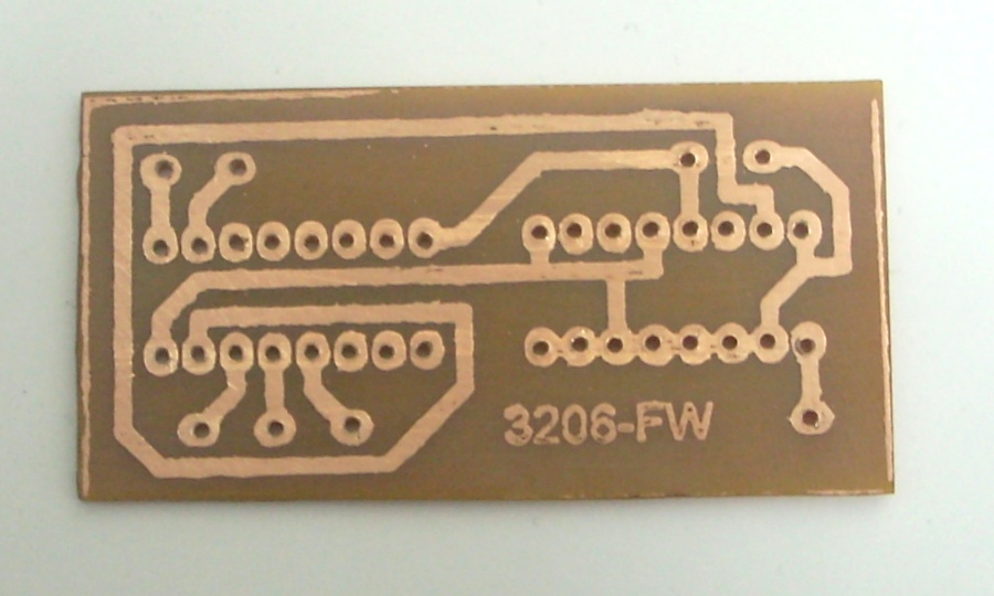
If you’re aiming for a professional finish and you’ve got the skills and materials to etch your own single sided printed circuit boards, here’s a neat PCB design that you can use to build your modification board:


The following PDF file contains the mirrored PCB artwork of the above board, ready to print and transfer. Download and print to photo grade paper using a laser printer, and don’t select any of the scaling of “fit to printer margins” options, the artwork is already at 1:1 scale.
Download PCB design (PDF, 33 KB)
Once you’ve etched your printed circuit board, install the components and solder the wires as shown in the following diagram:

Use color coded wires to avoid confusion. Make sure to install the chips the correct way around! Follow the labeling on top of the chips and respect the position of the black dot or mark on the corner.

Now your mod board is ready for installation.
Step 2: Installing the mod board
Now it’s time to install your fresh mod board into your FDS drive mechanism. You need to cut two traces and solder 8 wires to various points on the board. If you have installed a console modchip before, this step should be a piece of cake. Since the Famicom uses 1980s technology, the circuit board traces and solder points are big and clear to see, and therefore easy to solder on with basic to intermediate soldering skills.
- Remove the six Phillips screws that hold the FDS drive casing together. Flip the drive around and remove the top cover.
- Remove the four screws that hold the drive mechanism to the casing.
- Unplug the connector that joins the drive mechanism with the power board, taking note of its original orientation.
- Lift the drive mechanism out of the casing and set it aside.
With the drive mechanism out of the case, flip it around so that its bottom side faces up, and remove the three Phillips screws that hold the bottom metal plate together (one of the screws doesn’t hold the metal plate at all, don’t remove that one). Remove the metal plate to expose the circuit board underneath.

Rotate the disk drive mechanism so that the disk card slot faces away from you and the power board connector points at you (in the case of the above picture, rotate it 90 degrees counterclockwise).
In order to do a successful mod, you’ll need to familiarize yourself with this particular area of the circuit board, since we’ll be cutting a couple of traces and soldering several wires to it. Zoom in on the picture by clicking on it, compare it with your disk drive and make sure you can recognize the basic structures like the two parallel columns of solder points (which by the way is the Drive Controller IC). There’s no room for error!

You’ll need to cut two circuit board traces that link the original disk writing stage with the write head assembly. This will disable the original, crippled disk writing circuitry and allow our custom circuitry to take control.

Cut the marked traces in the exact same place that is detailed on the picture. If you cut them at another place you’ll also disconnect the pull-up resistors from the head assembly, which will prevent proper operation of the disk drive. Once the traces have been severed, use a multimeter or a magnifying glass to make sure that they’ve been completely disconnected from the chip.
Now take your mod board and solder each wire to its corresponding place indicated by the following picture. It helps to use color coded wires to avoid confusion.

Once again, triple check your work, look for unwanted solder bridges and wiring mistakes.
The end result should look like this:


The following step is optional but highly recommended. Take the bottom metal plate of the drive mechanism and cover the area directly underneath the 3206 chip with significant amounts of electrical tape. By doing this you’ll prevent possible short circuits between your soldered wires and the bottom metal plate. It also wouldn’t hurt to do the same to the bottom of the mod board, just in case.

With the wires firmly soldered into place, put the bottom metal plate back into place and route the wires through the small opening that the plate allows for. Make sure that the wires aren’t being pinched by the metal plate and screw it back together.

Slide the drive mechanism back into the casing, taking care for the mod board. Plug the power board connector into the drive mechanism, and place the mod board on an empty space inside the FDS drive casing, a good place for it should be one of the empty corners at the sides of the drive mechanism, making sure that it doesn’t short circuit with the metal parts of it. Use a piece of tape or a drop of hot glue to secure the board to the case and to avoid rattling.


Install the four screws that hold the drive mechanism, put the top casing back together and replace the six screws on the bottom. You’re done!
Step 3: Testing
With your FDS drive back together, it’s time to test your newly installed write modification. Hook up the FDS to your Famicom as usual, insert a disk that you don’t care about corrupting (just in case something is wrong), and turn everything on.
The disk drive should work just like before and boot up your game. Depending on the game, play a couple of levels and then lose all your lives, or create a new character/save file in order to call a data save routine. Select the SAVE option or confirm the creation of the new character, and wait for the disk drive to do its thing. If everything’s correct, the data should be saved successfully. If it does, congratulations! Your FDS drive is now copy unprotected! For the ultimate test, try rewriting a disk using your FDSLoadr setup.
If something didn’t behave like before, head on to the next section.
Troubleshooting
So it didn’t work as intended. Don’t worry; the mod is simple enough that the troubleshooting process is pretty straightforward. The problems that you’re likely to encounter can be divided into three categories:
- General erratic behavior
The disk drive isn’t recognizing an inserted disk, or it acts like a disk has been inserted regardless of a disk actually being in the drive, among other seemingly strange symptoms. These are most certainly related to incorrect wiring. Check that you’ve used the right solder points and that there are no unwanted solder blobs bridging stuff together. Do the same checks on your mod board. A good troubleshooting method is to remove the mod wires one by one until the symptoms disappear, that way you’ll quickly identify the culprit. If you didn’t put electrical tape on the bottom of the metal plate, now it’s a good time to do so.
- Disk reading errors (21, 22, 27)
Your disk drive seems to work fine but it won’t load any disks, giving out errors 21, 22 or 27. Once again this is mostly related to incorrect wiring, but also it can be related to mechanical issues, like your mod wires being pinched by the sharp metal edges of the bottom plate, the bottom plate not being fully screwed down or perfectly aligned, or maybe the wires are interfering with the drive’s spinning mechanism. The FDS drive is really finicky about this. Even a slightly misaligned bottom plate can affect disk reading. Recheck your wiring and your mounting.
- Disk loads fine but saving fails, producing Error 26
Everything seems to work fine, except for when you call a save routine in the game. It takes a really long time to save and it finally fails with an Err. 26. Upon reset you discover that no data has been saved to the disk. In this case, the circuit could be working fine but the write signals aren’t reaching the head assembly, or the whole mod board isn’t working at all. Again the most likely cause is incorrect wiring but this one is a more particular failure mode. Check that the traces that you’ve cut are fully disconnected from the original circuit, and that you’ve soldered the write head wires to the correct spots on the board.
A final word of caution
Incorrect wiring can cause disk data corruption, because the write disable circuitry may not be operating properly and allowing the write heads to work at undesired times if the , and signals aren’t properly connected. If you can’t get it to work, as a last resort try undoing the mod completely and see if your disk still loads up to rule out data corruption. If you disk won’t boot up anymore even without any trace of the mod, it has been corrupted by undesired writing. Don’t use a disk that you care about for testing purposes, and don’t try out other disks if the first one doesn’t boot up – you could be corrupting them all!