Article
It is a well known fact that Nintendo made two revisions of the drive controller chip inside the Famicom Disk System 3″ drive. The FD7201 is the first release which doesn’t contain any copy protection feature whatsoever. The FD3206 is an improved version of the 7201 which forbids you from rewriting the entire Disk Card.
What is not widely known, even inside Famicom collector and technical circles is that there is another copy protection measure inside Famicom Disk System units besides the drive controller chip. This little-known fact has caused many frustrations among Famicom enthusiasts who own a FDS with a 7201 drive chip, built an FDSLoadr cable and then wonder why they can’t get the disk writing part to work, when everything seems correct.
First off, let’s take a look inside the Famicom Disk System drvie (HVC-022):
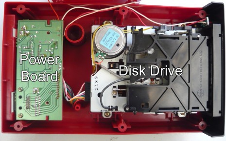
The Famicom Disk System unit consists of two main parts: The custom Mitsumi 3″ Quick Disk drive mechanism on the right, and a Printed Circuit Board on the left which we will call the Power Board from now on. The well-known Drive Controller Chip (either FD7201 or FD3206) resides in the drive mechanism on the right.
We’re going to focus on the Power Board. As the name implies, this circuit board supplies power to the drive mechanism either from batteries or the AC adapter, it contains an electronically switched 2-way power supply which redirects power from any of these two sources to the drive motor at the RAM Adapter’s request. It also carries all of the data and control signals from the RAM Adapter connector on the back of the unit to the Mitsumi drive mechanism.
Nintendo made five revisions of the Power Board circuit, which are labeled FMD-POWER-01 to FMD-POWER-05. The most notable difference between earlier and later revisions of the board is their physical size (higher revisions tend to be larger), but the most important change is the addition of a copy protection circuit to the later revisions of this board. Presumably, Nintendo added these copy protection measures to their Power Boards while they redesigned the Drive Controller Chip as an intermediate means to thwart piracy, and also to strengthen the overall security of the system, by providing two copy-protection paths instead of just one.
This explains why you can have a FDS drive with a 7201 Drive Chip and not being able to rewrite disks. If your drive sports one of the copy-protected Power Boards, you won’t be able to rewrite disks even if you have a drive mechanism with the “good” 7201 chip.
Fortunately, the Power Board protection is a lot easier to defeat than the Drive Chip protection inside the drive mechanism. You need minimal soldering skills and the ability to remove components, break circuit board traces and solder jumper wires between points. First you need to identify which Power Board revision your drive comes with to see if it needs any modification, and if it needs one, the exact steps to perform it (every Power Board revision is different from the last one).
Identifying your Power Board Revision
- First, open up your FDS Unit (HVC-022) by removing the six Phillips screws on the bottom of the unit.
- Flip the drive and carefully remove the top cover.
- Remove the two Phillips screws holding the battery compartment to the system case.
- Set the battery compartment aside and remove the screws holding the Power Board to the case.
- Carefully remove the Power Board from the case and flip it over so that the component side is facing you.
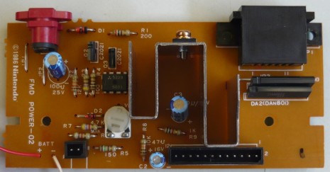
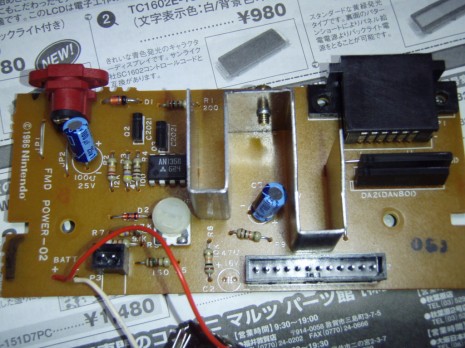
Here is a typical Power Board. Size and component placement may vary. This specific one is the FMD-POWER-02 board. Look around the board for the copyright notice ©198X Nintendo and the code FMD-POWER-XX, where XX is a number between 01 and 05. Once you identify this number, you can proceed to the next section.
Nintendo Power Board Revisions List:
- FMD-POWER-01: First revision, no protection. Doesn’t need modification.
- FMD-POWER-02: Mixed. Some boards have protection while others do not. Might need a simple modification. Check the next section for more details.
- FMD-POWER-03: Unknown. Presumed to be unprotected or similar to FMD-POWER-02. If you have one of these, please contact Famicom World staff.
- FMD-POWER-04: Copy-protected board. Needs modification.
- FMD-POWER-05: Copy-protected board. Needs modification.
Power Board Modification Procedures
- FMD-POWER-01:
No Picture
This board doesn’t have any copy protection measures built-in. If you have one of these, you’re lucky!.
- FMD-POWER-02:
There are two versions of this board:

This version doesn’t contain any copy protection measures. Consider yourself lucky!
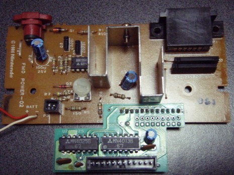
This one contains an added green daughter-board. This daughter-board contains the write lockout logic which forbids you from rewriting Disk Cards. Fortunately removing it is really easy. You only need to remove this board altogether and make your board look like the first FMD-POWER-02 version above.

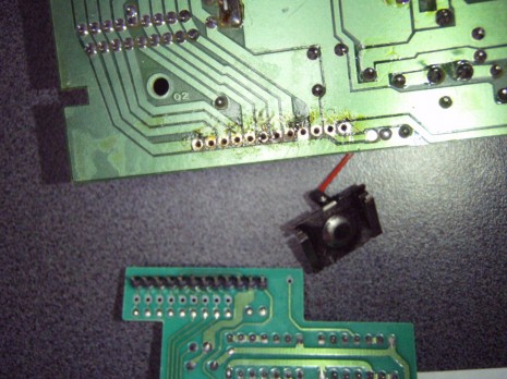
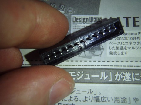
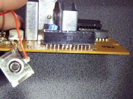
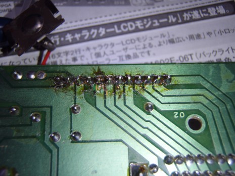

Many thanks to Michael Kennedy (mikek400@comcast.net) for these detailed pictures.
- FMD-POWER-03:
No Picture
Unknown. Presumed to be unprotected or similar to FMD-POWER-02. If you have one of these, please contact Famicom World staff.
- FMD-POWER-04:
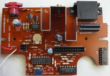
At first glance the increased size of this board immediately stands out. All of the additional components on the bottom side are responsible for the copy protection logic. You don’t need to remove them all, it’s possible to disable the circuit and route around it, which is considerably easier. Here’s the modification procedure for this board:
First, you need to remove the component labeled JP14. You can desolder it or cut it with a pair of fine pliers, it doesn’t matter: you just need it out of there. Removing this component disables the copy protection circuit completely. Next, you need to route the write signal around the now disabled circuit so that it can reach the drive mechanism.
Now use your soldering iron and link the points A and B together using a piece of wire. The gap is short enough to use a small piece of solder as the wire link, provided you don’t short out something else. I’ve also labeled the solder points for JP14 to make desoldering easier.
Once you removed JP14 and linked the points, you’re done! Enjoy your unprotected Power Board!
- FMD-POWER-05:

This is the last revision of the FDS Power Board, and not surprisingly, the hardest to mod. Fortunately it’s only a couple of extra easy steps longer than the FMD-POWER-04 mod.
You need to remove two jumper wires, cut two circuit board traces and solder two wires between contact points.
First, you need to remove two jumper wires. I recommend you to desolder them instead of just using pliers to snip them off. One of them is buried between the two black rectangle-shaped components near the RAM Adapter connection. You can bend those outwards a little to expose the jumper wire underneath. I’ve marked the solder points for both of them on the next picture to make desoldering easier.
Now you need to cut two circuit board traces which are marked with red dashes on the picture. This will disable the copy protection mechanism. Use a sharp object like an X-Acto knife or a jeweler’s screwdriver to sever them. Make sure they’re completely cut and that no electrical connection exists between them. Next, solder two wire links like the blue ones marked in the picture. This will route the write signals back where they belong: the drive mechanism.
And that’s it! Now reassemble your drive and happy disk writing!
